오늘은 FP6161-1.5MHz, 1A Synchronous Step-Down Regulator에 대한 고찰을 해 보겠습니다.
FP6161은 1.5MHz, 1A Synchronous Step-Down Regulator로 아래와 같은 특성을 지니고 있습니다.
FP6161는 Package가 DFN도 있지만, SOT23-5L인 FP6161KR-LF-ADJ가 제일 사용하기좋습니다.
먼저 가격도 DFN보다 저렴하며, Board에서 Test를 하거나, Debugging할때 Chip의 Pin이 밖으로 나와있기때문에
DFN보다 편리하며, 대부분의 고객이 SOT23-5L Package를 사용하기에 납기에도 편리합니다.
The FP6161 is a high efficiency current mode synchronous buck PWM DC-DC regulator.
The internal generated 0.6V precision feedback reference voltage is designed for low output voltage.
Low RDS (ON) synchronous switch dramatically reduces conduction loss.
To extend battery life for portable application, 100% duty cycle is supported for low-ropout operation.
Shutdown mode also helps saving the current consumption.
The FP6161 is packaged in DFN-6L, SOT23-5L, and TSOT23-5L to reduce PCB space.
-
Synchronous Buck Converter
-
Input Voltage Range: 2.5 to 5.5V
-
Precision Feedback Reference Voltage: 0.6V (±2%)
-
Output Current: 1A (Max.)
-
Duty Cycle: 0~100%
-
Internal Fixed PWM Frequency: 1.5MHz
-
Low Quiescent Current: 100μA
-
Built -in PMOS & NMOS, No Schottky Diode Required
-
Light Load Power Saving Mode, High Efficiency
-
Over Current Protection(OCP), Short Circuit Protection(SCP), Over Temperature Protection(OTP)
-
Built-in Soft Start
-
Current Mode Operation
-
Over Temperature Protection
-
Package: DFN-6L (2x2mm), SOT23-5L, TSOT23-5L
Function Description
Control Loop
The FP6161 is a high efficiency current mode synchronous buck regulator.
Both the main (P-channel MOSFET) and synchronous (N-channel MOSFET) switches are built internally.
With current mode operation, the PWM duty is controlled both by the error amplifier output and the peak
inductor current.
At the beginning of each cycle, the oscillator turn on the P-MOSFET switch to source current from VIN to SW output.
Then, the chip starts to compare the inductor current with the error amplifier output.
Once the inductor current is larger than the error amplifier output, the P-MOSFET switch is turned off.
When the load current increases, the feedback voltage FB will slightly drop.
This causes the error amplifier to output a higher current level until the prior mentioned peak inductor current reach the same level.
The output voltage then can be sustained at the same.
When the top P-MOSFET switch is off, the bottom synchronous N-MOSFET switch is turned on.
Once the inductor current reverses, both top and bottom MOSFET will be turn off to leave the SW pin into high impedance state.
The FP6161’s current mode control loop also includes slope compensation to suppress sub-harmonic oscillations at high duty cycles.
This slope compensation is achieved by adding a compensation ramp to the inductor current signal.
LDO Mode
The FP6161’s maximum duty cycle can reach 100%.
That means the driver’s main switch is turn on through out whole clock cycle.
Once the duty reaches 100%, the feedback path no longer controls the output voltage.
The output voltage will be the input voltage minus the main switch voltage drop.
Over Current Protection
FP6161 limits the peak main switch current cycle by cycle.
When over current occurs, chip will turn off the main switch and turn the synchronous switch on until next cycle.
Short Circuit Protection
When the FB pin drops below 300mV, the chip will tri-state the output pin SW automatically.
After 300us rest to avoid over heating, chip will re-initiate PWM operation with soft start.
Thermal Protection
FP6161 will shutdown automatically when the internal junction temperature reaches 150℃ to
protect both the part and the system.
Application Information
Input Capacitor Selection
The input capacitor must be connected to the VIN pin and GND pin of FP6161 to maintain steady
input voltage and filter out the pulsing input current.
The voltage rating of input capacitor must be greater than maximum input voltage plus ripple voltage.
In switch mode, the input current is discontinuous in a buck converter.
The source current waveform of the high-side MOSFET is a square wave.
To prevent large voltage transients, a low ESR input capacitor sized for the maximum RMS current must be used.
Inductor Selection
The value of the inductor is selected based on the desired ripple current.
Large inductance gives low inductor ripple current and small inductance result in high ripple current.
However, the larger value inductor has a larger physical size, higher series resistance, and / or lower saturation current.
In experience, the value is to allow the peak-to-peak ripple current in the inductor to be 10%~20% maximum load current.
Output Capacitor Selection
The output capacitor is required to maintain the DC output voltage.
Low ESR capacitors are preferred to keep the output voltage ripple low.
In a buck converter circuit, output ripple voltage is determined by inductor value, switching frequency, output capacitor value and ESR.
Using Ceramic Input and Output Capacitors
Care must be taken when ceramic capacitors are used at the input and the output.
When a ceramic capacitor is used at the input and the power is supplied by a wall adapter through long wires, a
load step at the output can induce ringing at the input, VIN.
At best, this ringing can couple to the output and be mistaken as loop instability.
At worst, a sudden inrush current through the long wires can potentially cause a voltage spike at VIN,
which may large enough to damage the part.
When choosing the input and output ceramic capacitors, choose the X5R or X7R specifications.
Their dielectrics have the best temperature and voltage characteristics of all the ceramics for a given value and size.
예로서 아래와 같은 Application이 있습니다.
Vin=5V, Vout=3.3V/1A
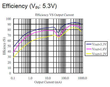
Frequency=1.5MHz, Efficiency=89.2%, Output Ripple=22mV, Temperature IC1=55℃, L1=43℃

아래는 spec sheet의 응용 회로도입니다.
PC Board Layout Checklist
1. The power traces, consisting of the GND, SW and VIN trace should be kept short, direct and
wide.
2. Place CIN near VIN pin as closely as possible to maintain input voltage steady and filter out the
pulsing input current.
3. The resistive divider R1 and R2 must be connected to FB pin directly and as closely as possible.
4. FB is a sensitive node. Please keep it away from switching node, SW. A good approach is to
route the feedback trace on another PCB layer and have a ground plane between the top and
feedback trace routing layer. This reduces EMI radiation on to the DC-DC converter its own
voltage feedback trace.
5. Keep the GND plates of CIN and COUT as close as possible. Then connect this to the ground
plane (if one is used) with several vias. This reduces ground plane noise by preventing the
switching currents from circulating through the ground plane. It also reduces ground bounce at
FP6161 by giving it a low impedance ground connection.
'끝없는 Power를 위하여' 카테고리의 다른 글
| WDKOREA is WDKOREA (0) | 2021.01.02 |
|---|---|
| FP6165-1.5MHz, 3A Synchronous Step-Down Regulator에 대한 고찰 (0) | 2020.12.31 |
| FP6193-3A, 23V, 340KHz Synchronous Step-Down Converter에 대한 고찰 (0) | 2020.12.29 |
| FP8208-3.5A Synchronous Switch-Mode 1-Cell Li-Ion Battery Charger에 대한 고찰 (0) | 2020.12.26 |
| SP687-X2 Capacitor Discharge IC에 대한 고찰 (0) | 2020.12.24 |