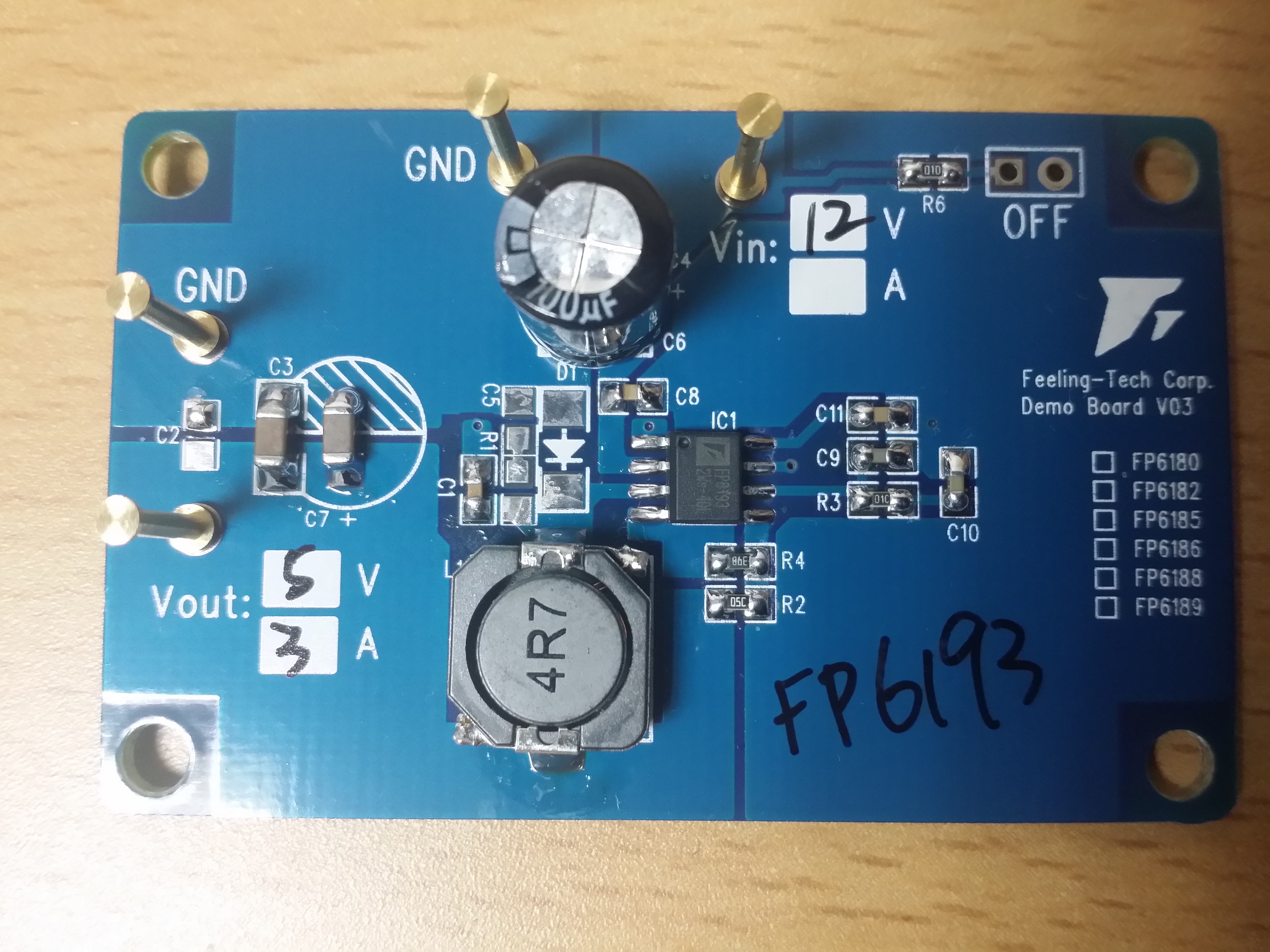
오늘은 FP6193-3A, 23V, 340KHz Synchronous Step-Down Converter에 대한 고찰을 해 보겠습니다.
FP6193-3A은 23V, 340KHz Synchronous Step-Down Converter로 아래와 같은 특성을 지니고 있습니다.
DCDC Converter PCB Artwork 할 때는 PCB Pattern이 상당히 중요합니다.
기본적으로 Switching 하는 Chip에 영향을 주지 않는 방향으로 PCB Pattern을 만들어야 하는데, 영향을 미친 경우는 Switching 파형을 오실로스코프로 보면, 파형이 Unbalance 나고, Noise가 발생하여 발진 소리가 나고, 제대로 된 Switching 파형이 아님을 쉽게 볼 수 있습니다.
이런 부분이 어렵습니다. Digital Logic처럼, 단순히 Pattern만을 연결하면 위와 같이 잘 동작하지 않을 수 있습니다.
이때, COMP Pin에 있는 R3, C9, C10의 값을 조정하여 Switching파형을 안정화시킬 수 있습니다.
FP6193은 아래와 같은 특성을 지니고 있습니다.
The FP6193 is a synchronous buck regulator with integrated two 85mΩ power MOSFETs.
It achieves 3A continuous output current over a wide input supply range with excellent load and line regulation.
Current mode operation provides fast transient response and eases loop stabilization.
The device includes cycle-by-cycle current limiting and thermal shutdown protection.
The FP6193 requires a minimum number of readily available external components to complete a 3A buck regulator solution.
-
3A Output Current
-
85mΩ Internal Power MOSFET Switches
-
Stable with Low ESR Output Ceramic Capacitors Up to 93% Efficiency
-
Programmable Soft-Start
-
Fixed 340KHz Frequency
-
Thermal Shutdown
-
Cycle-by-Cycle Over Current Protection
-
Wide 4.75V to 23V Operating Input Range
-
Output Adjustable From 0.923V to 20V
-
Available SOP-8L (EP) Package
-
Input Under Voltage Lockout
Function Description
The FP6193 is a synchronous current-mode buck regulator.
It regulates input voltages from 4.75V to 23V down to an output voltage as low as 0.923V,
and is able to supply up to 3A of load current.
The FP6193 uses current-mode control to regulate the output voltage.
The output voltage is measured at FB through a resistive voltage divider and amplified by the internal error amplifier.
The output current of the tranconductance error amplifier is presented at COMP where a network compensates the regulation
control system.
The voltage at COMP is compared to the switch current measured internally to control the output voltage.
The converter uses internal n-channel MOSFET switches to step-down the input voltage to the regulated output voltage.
Since the MOSFET requires a gate voltage greater than the input voltage, a boost capacitor connected
between SW and BS drives the gate.
The capacitor is charged from the internal regulator when the SW pin is low.
Output Voltage (VOUT)
The output voltage is set using a resistive voltage divider from the output voltage to FB.
Enable Mode / Shutdown Mode
Drive the EN Pin to ground to shutdown the FP6193.
Shutdown forces the internal power
MOSFETs off, turns off all internal circuitry.
The EN Pin rising threshold is 1.5V (typ), and hysteresis is
300mV. For automatic startup application, pull up the EN pin with 100KΩ resister.
Boost High-Side Gate Drive (BST)
Since the MOSFET requires a gate voltage greater than the input voltage, connect a flying bootstrap capacitor between SW and BS to provide the gate-drive voltage to the high-side n-channel MOSFET switch.
The capacitor is alternately charged from the internal regulator.
On startup, an internal low-side switch connects SW to ground and charges the BST capacitor to internal regulated voltage.
Once the BST capacitor is charged, and the internal low-side switch is turned off, the BST capacitor
voltage provides the necessary enhancement voltage to turn on the high-side switch.
Thermal Shutdown Protection
The FP6193 features integrated thermal shutdown protection.
When the IC junction temperature exceeds +150°C, thermal shutdown protection will be triggered.
The internal power MOSFET is then turned off to limit the device power dissipation (PD).
Once thermal shutdown occurs, this device can go back to normal operation until the junction temperature drops
below +100°C approximately.
Application Information
Input Capacitor Selection
The input current to the step-down converter is discontinuous, therefore a capacitor is required to
supply the AC current to the step-down converter while maintaining the DC input voltage.
Use low ESR capacitors for the best performance. Ceramic capacitors are preferred, but tantalum or low-ESR
electrolytic capacitors may also suffice.
The input capacitor can be electrolytic, tantalum or ceramic.
When using electrolytic or tantalum capacitors, a small, high quality ceramic capacitor, i.e. 0.1μF, should be placed as close to the IC as possible.
When using ceramic capacitors, make sure that they have enough capacitance to provide sufficient charge to prevent
excessive voltage ripple at input.
Inductor Selection
The inductor is required to supply constant current to the output load while being driven by the
switched input voltage.
A larger value inductor will result in less ripple current that will result in lower output ripple voltage. However,
the larger value inductor will have a larger physical size, higher series resistance, and / or lower saturation current.
A good rule for determining the inductance to use is to allow the peak-to-peak ripple current in the inductor
to be approximately 30% of the maximum switch current limit.
Output Capacitor Selection
The output capacitor is required to maintain the DC output voltage.
Ceramic, tantalum, or low ESR electrolytic capacitors are recommended.
Low ESR capacitors are preferred to keep the output voltage ripple low.
예로서 아래와 같은 Application이 있습니다.
1. Vin=12V, Vout=5V/3A
Efficiency=86.65%, Temperature IC1=91℃, L1=64℃
Frequency=356kHz, Output Ripple=48mV
2. Vin=12V, Vout=9V/1.8A
Efficiency=95%, Temperature=59℃
3. Vin=15V, Vout=12V/1.5A
Efficiency=95.5%, Temperature=55℃
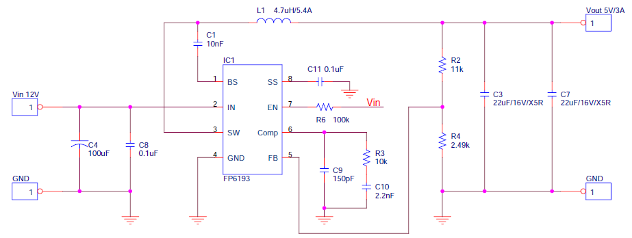
아래는 spec sheet의 응용 회로도입니다.
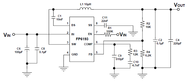
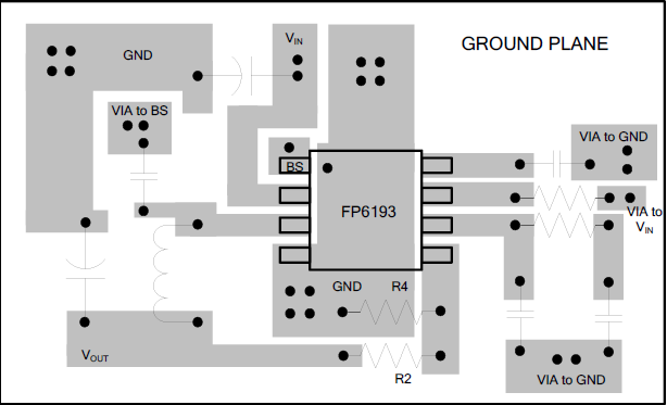
PC Board Layout Checklist
1. The power traces, consisting of the GND trace, the SW trace and the VIN trace should be kept short, direct and wide.
2. Place CIN near IN Pin as closely as possible. To maintain input voltage steady and filter out the pulsing input current.
3. The resistive divider R2 and R4 must be connected to FB pin directly as closely as possible.
4. FB is a sensitive node. Please keep it away from switching node, SW. A good approach is to route the feedback trace
on another layer and to have a ground plane between the top layer and the layer on which the feedback trace is routed.
This reduces EMI radiation on to the DC-DC converter’s own voltage feedback trace.

'끝없는 Power를 위하여' 카테고리의 다른 글
| FP6165-1.5MHz, 3A Synchronous Step-Down Regulator에 대한 고찰 (0) | 2020.12.31 |
|---|---|
| FP6161-1.5MHz, 1A Synchronous Step-Down Regulator에 대한 고찰 (0) | 2020.12.31 |
| FP8208-3.5A Synchronous Switch-Mode 1-Cell Li-Ion Battery Charger에 대한 고찰 (0) | 2020.12.26 |
| SP687-X2 Capacitor Discharge IC에 대한 고찰 (0) | 2020.12.24 |
| FP6153-3A, 36V,Synchronous Step-Down Converter에 대한 고찰 (0) | 2020.12.24 |