오늘은 FP5207-Non-Synchronous PWM Boost Controller에 대한 고찰을 해 보겠습니다.
FP5207은 Boost Controller로 아래와 같은 특성을 지니고 있습니다.
외부에 N-ch MOSFET를 이용해서 High Power DCDC converter를 만들 수 있습니다.
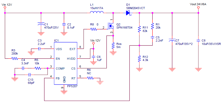
아래의 회로도를 보면 충분히 이해가 될 것 같습니다.
The FP5207 is boost topology switching regulator for wide operating voltage applications.
It provides built-in gate driver pin for driving external N-MOSFET.
The non-inverting input of error amplifier connects to a 1.2V precision reference voltage.
It has programmable switching frequency set by external resistor, and programmable inductor peak current limit connects a resistor from CS to GND.
Current mode control and external compensation network make is easy and flexible to stabilize the system.
The FP5207 is available in the small footprint SOP-8L(EP) package to fit in space-saving PCB layout for application fields.
-
Asynchronous Boost Controller
-
Input Start-up Voltage:2.8V
-
Input Supply Voltage:5 to 24V
-
Feedback Reference Voltage:1.2V(± 2%)
-
Shutdown Current: <3μA
-
Duty Cycle:90%(max.)
-
Programmable Switching Frequency:100KHz~1000KHz
-
Input Under Voltage Protection:Control EN Pin
-
Switching MOSFET Over Current Protection (OCP;(100mV Current Sense Voltage, Limit Driver NMOS Peak Current))
-
Over Temperature Protection (OTP)
-
EXT Pin:Gate Driver 8V/0.9Ω Push-Pull Resistance
-
Package:SOP-8L(EP)
Function Description
Operation
The FP5207 is current mode boost controller. It operates with pulse width modulation (PWM).
The internal resistive divider provides 1.2V reference for the error amplifier.
It changes to PSM mode when the output is light load. In PSM mode, it can reduce switching lose to raise efficiency, but the
output ripple is bigger.
Soft Start Function
After the IC is enabled, the output of error amplifier is clamped by the internal soft-start function, which causes PWM pulse width increasing slowly and thus reducing input surge current during power on.
Oscillator
The oscillator frequency can be set from 100KHz to 1000KHz by external resistance. Acceptable
resistance values range from 220KΩ to 17KΩ.
The frequency is 150KHz when the resistance is unconnected.
Enable Mode / Shutdown Mode
The EN voltage is lower than 1.3V to shutdown it.
In shutdown mode, to turn off circuitry includes EXT signal, VDS voltage, and supply current of HVDD reduces less than 3μA.
The EN hysteresis voltage is 0.2V. HVDD voltage may be lower than 5V, it can’t use a resistive divider to set UVLO threshold.
For instance, input voltage is from 3V to 4.2V, HVDD pin connects to output 12V, when UVLO is triggered to shut down FP5207, HVDD and output are approximately input voltage.
If the applications don’t need to set UVLO, the EN connects to input voltage through resistance 200KΩ, and EN internal clamping circuit limit VEN is under 5.5V.
Current Sense Control
External switching MOSFET is turned on inductor current flows across the current sense resistor
to generate VCS.
VCS provides part of current mode control loop. Internal leading-edge blanking is provided to prevent premature
turn off the switching MOSFET in each switching cycle.
Current Limit Setting Resistor (RCS)
RCS is connected between CS pin and ground, its calculation formula is as below.
Where 0.085V is minimum threshold voltage of current sense, ILp is peak inductor current, and the factor 1.3 provides a
30% margin for tolerances.
Thermal Shutdown Protection
The IC will shut down automatically when the internal junction temperature exceeds +150°C.
The device can restart until the junction temperature drops below +120°C approximately.
Application Information
Inductor Selection
The Inductance value is decided based on different condition.
3.3μH to 47uH inductance value is recommended for general application circuit.
There are three important inductor specifications, DC resistance, saturation current and core loss.
Low DC resistance has better power efficiency.
Capacitor Selection
Output capacitor is required to maintain the DC voltage during switching.
Low ESR capacitors are preferred to reduce the output voltage ripple.
Ceramic capacitor of X5R and X7R are recommended, which have low equivalent series resistance (ESR)
and wider operation temperature range.
Diode Selection
Schottky diodes with fast recovery times and low forward voltages are recommended.
Ensure the diode average and peak current rating exceed the average output current and peak inductor current.
In addition, the diode’s reverse breakdown voltage must exceed the output voltage.
Output Voltage Programming
The output voltage is set by a resistive voltage divider from the output voltage to FB.
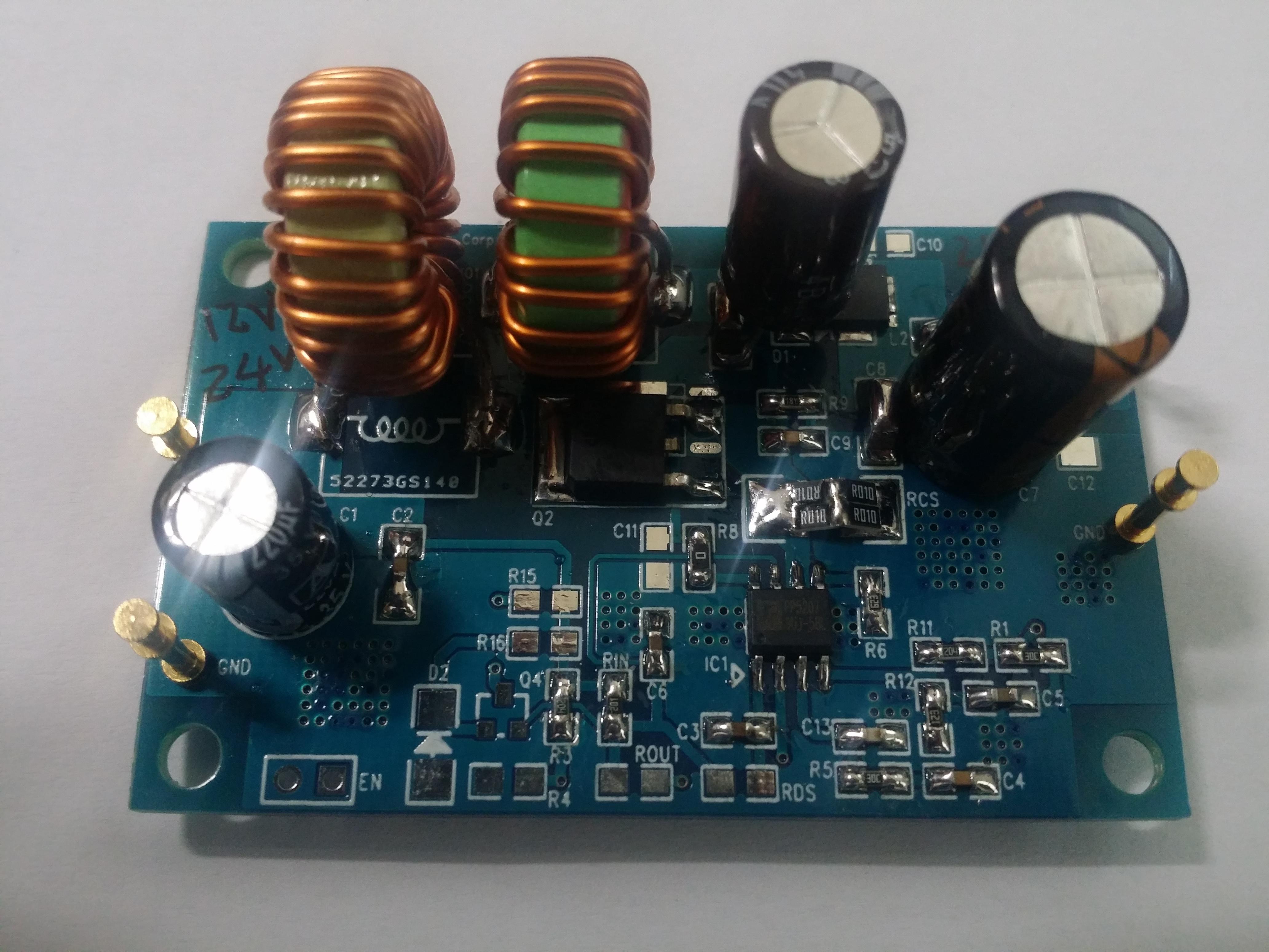
예로서 아래와 같은 Application이 있습니다.
아래 Application Demo Board는 SEPIC(Buck-Boost) Topology입니다, 따라서 아래와 같은 Test 결과를 갖습니다.
Vin=12V, Vout=21V/1.5A
Frequency=300kHz, Efficiency=90.2%, Output Ripple=290mV, Temperature Q2=77℃, L1=68℃, L3=58℃, D1=77℃
Vin=24V, Vout=21V/1.5A
Frequency=300kHz, Efficiency=88.9%, Output Ripple=220mV, Temperature Q2=77℃, L1=89℃, L3=76℃, D1=78℃
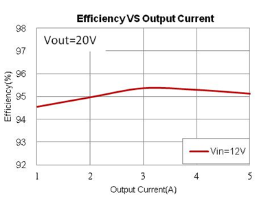
또다른 Application입니다.

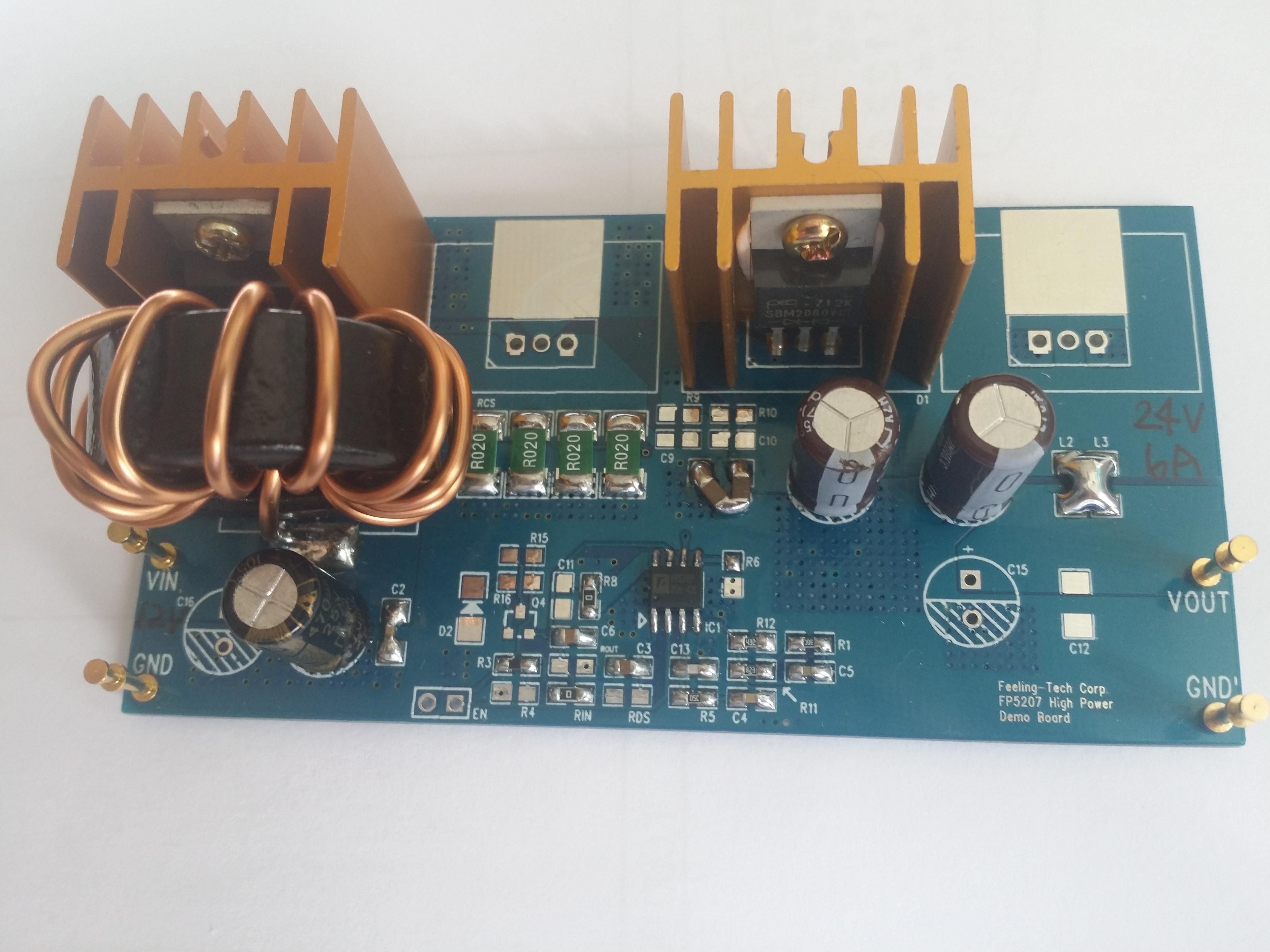

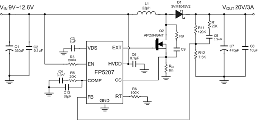
아래는 spec sheet의 응용 회로도입니다.


아래는 spec sheet의 응용 회로의 PCB Suggestion Layout입니다, PCB artwork시 고려해야 할 내용입니다.
힘드시면, 그냥 똑같이 하시도 됩니다.
1. The power traces, consisting of the GND trace, the MOS drain trace and the Vin trace should be kept short, direct and wide.
2. Layout switching node MOS drain, inductor and schottky diode connection traces wide and short to reduce EMI.
3. Place C6 nearby HVDD pin as closely as possible to maintain input voltage steady and filter noise.
4. Resistive divider R11 and R12 must be connected to FB and GND pin directly and as closely as possible.
5. FB is a sensitive node. Please keep it away from switching node, MOS drain.
6. The GND of the Q2, C1, C2, C7 and C8 should be connected close and together directly to a ground plane.
7. RCS must be connected to CS and GND pin directly and as closely as possible.
8. The output capacitor C7 and C8 should be connected close and together directly to the ground of Rcs.
9. The X5R and X7R of ceramic capacitors are recommended to choose.
10. R9 and C9 are added for reducing EMI (Electromagnetic Interference).
