오늘은 FP6298-Low-Noise 4.5A Step-Up Current Mode PWM Converter에 대한 고찰을 해 보겠습니다.
FP6298은 DCDC Boost Converter로서 아래와 같은 특성을 지니고 있습니다.
내부 Switching Current가 4.5A로서, 1 Cell Li-Ion Battery 입력을 사용해서 5V/2A까지는 충분히 출력을 내는 IC입니다.
비교적 주변회로가 간단해서 편리합니다.
The FP6298 is a current mode boost DC-DC converter. It is PWM circuitry with built-in 0.08Ω power MOSFET make this regulator highly power efficient.
The internal compensation network also minimizes as much as 6 external component counts.
The non-inverting input of error amplifier connects to a 0.6V precision reference voltage and internal soft-start function can reduce the inrush current.
The FP6298 is available in the SOP-8L(EP) package and provides space-saving PCB for the application fields.
-
Adjustable Output up to 10V
-
Internal Fixed PWM frequency: 500KHz
-
Precision Feedback Reference Voltage: 0.6V (±2%)
-
Internal 0.08Ω, 4.5A, 12V Power MOSFET
-
Shutdown Current: 0.1μA
-
Over Temperature Protection
-
Over Voltage Protection
-
Adjustable Over Current Protection: 0.5A ~ 4.5A
-
Package: SOP-8L(EP)
As function Description,
Operation
FP6298 is a current mode boost converter.
The switching frequency is 500KHz and operates with pulse width modulation (PWM). Build-in 12V / 4.5A MOSFET provides a high output voltage.
The control loop architecture is peak current mode control; therefore slope compensation circuit is added to the current signal to allow stable operation for duty cycles larger than 50%.
Soft Start Function
Soft start circuitry is integrated into FP6298 to avoid inrush current during power on.
After the IC is enabled, the output of error amplifier is clamped by the internal soft-start function, which causes
PWM pulse width increasing slowly and thus reducing input surge current.
Current Limit Program
A resistor between OC and GND pin programs peak switch current. The resistor value should be between 26k to 500k.
The current limit will be set from 4.5A to 0.5A. Keep traces at this pin as short as possible. Do not put capacitance at this pin.
Over Temperature Protection (OTP)
FP6298 will turn off the power MOSFET automatically when the internal junction temperature is over 150°C.
The power MOSFET wake up when the junction temperature drops 30°C under the OTP threshold temperature.
Over Voltage Protection (OVP)
In some condition, the resistive divider may be unconnected, which will cause PWM signal to
operate with maximum duty cycle and output voltage is boosted higher and higher.
The power MOSFET will be turned off immediately, when the output voltage exceeds the OVP threshold level.
The FP6298’s OVP threshold is 12V.
As application Information
Inductor Selection
Inductance value is decided based on different condition. 3.3uH to 4.7μH inductor value is recommended for general application circuit.
There are three important inductor specifications, DC resistance, saturation current and core loss.
Low DC resistance has better power efficiency.
Capacitor Selection
The output capacitor is required to maintain the DC voltage.
Low ESR capacitors are preferred to reduce the output voltage ripple.
Ceramic capacitor of X5R and X7R are recommended, which have low equivalent series resistance (ESR) and wider operation temperature range.
Diode Selection
Schottky diodes with fast recovery times and low forward voltages are recommended.
Ensure the diode average and peak current rating exceed the average output current and peak inductor current.
In addition, the diode’s reverse breakdown voltage must exceed the output voltage.
Output Voltage Programming
The output voltage is set by a resistive voltage divider from the output voltage to FB.
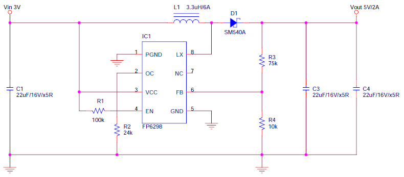
아래 사진은 Application Demo Board입니다, 회로가 아주 간단합니다.
Vin=3V, Vout=5V/2A
Frequency=495kHz, Efficiency=84%
Output Ripple=110mV, Temperature IC1=75℃, L1=65℃, D1=83℃

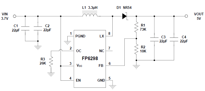
아래는 spec sheet의 응용 회로도입니다.
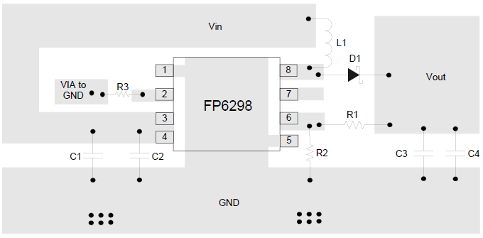
PCB artwork시에 고려해야할 부분입니다.
1. The power traces, consisting of the GND trace, the LX trace and the VCC trace should be kept short, direct and wide.
2. LX, L and D switching node, wide and short trace to reduce EMI.
3. Place CIN near VCC pin as closely as possible to maintain input voltage steady and filter out the pulsing input current.
4. The resistive divider R1 and R2 must be connected to FB pin directly as closely as possible.
5. FB is a sensitive node. Please keep it away from switching node, LX.
6. The GND of the IC, CIN and COUT should be connected close together directly to a ground plane.
7. Don’t pull the Vout back to the FP6298’s Vcc pin. When the system receives the noise, it will lead to Vout ripple too high and over the absolute maximum rating of the Vcc pin.
'끝없는 Power를 위하여' 카테고리의 다른 글
| FP6168-Dual 1.5MHz, 1A Synchronous Step-Down Regulator에 대한 고찰. (0) | 2021.01.11 |
|---|---|
| FP5207-Non-Synchronous PWM Boost Controller에 대한 고찰 (0) | 2021.01.07 |
| FP6296-10A Current Mode Non-Synchronous PWM Boost Converter에 대한 고찰 (0) | 2021.01.04 |
| FP6276B-500kHz 6A High Efficiency Synchronous PWM Boost Converter에 대한 고찰 (0) | 2021.01.04 |
| WDKOREA is WDKOREA (0) | 2021.01.02 |