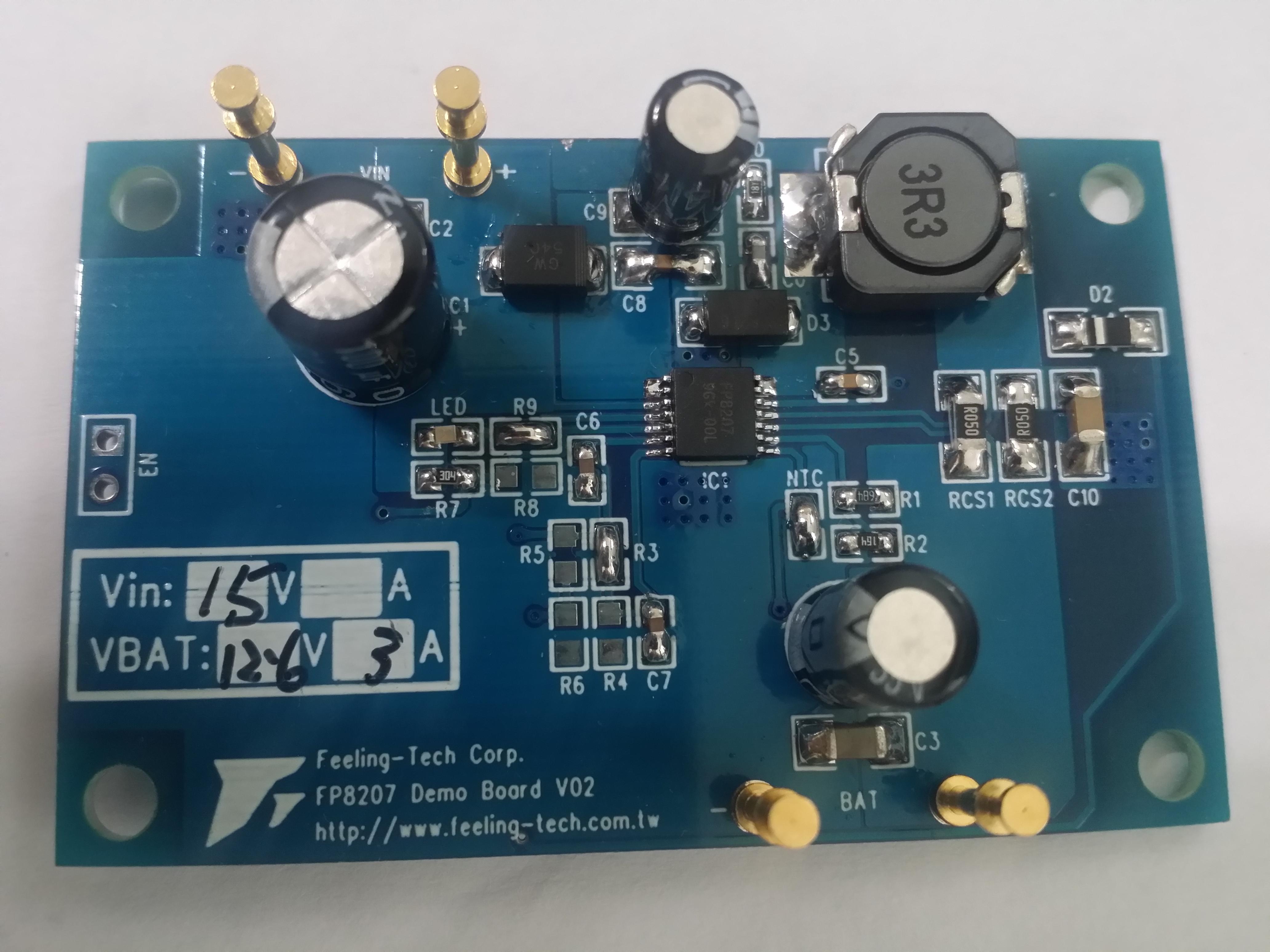
오늘은 FP8207-16V 3A Multi-Cell Battery Switching Charger에 대한 고찰을 해 보겠습니다.
보통 Charger Chip의 특성은 1 cell, 또는 2 cell인데, 이것은 3 Cell이며, 충전 전류도 3A까지 충전할 수 있어 큰 용량입니다. 요즘은 휴대용 제품 중에서 짧은 시간 내에 충전해서 사용하려는 고객의 욕구가 있어 충전 전류가 올라가는데 적합한 Chip인 것 같습니다.
FP8207은 16V 3A Multi-Cell Battery Switching Charger로 아래와 같은 특성을 지니고 있습니다.
The FP8207 is a 4.9V~16V input voltage, 3A multi cell synchronous step-down switching charger
with few external components, FP8207 is well suited for a wide range of portable applications.
Charging current can be programmed by an external current sensing resistor. With 500KHz switching
frequency. The FP8207 employs a 2.4V float voltage feedback reference, so any desired battery float
voltage up to 12.6V can be programmed with a resistor divider. Other features include UVLO,
automatic recharge, charge status indicators and battery temperature monitor.
-
Wide Input Voltage Range: 4.9V to 16V
-
Up to 3A Programmable Charge Current
-
Resistor Programmable Battery Float Voltage Range: 4.1V to 12.6V
-
Preset Charge Voltage with ±1% Accuracy
-
Automatic Recharge
-
Fix 500KHz Switching Frequency
-
Support 94% Duty Cycle
-
Thermal Regulation
-
Charge Status Indicators for No Battery and Charge Failure Display
-
Available TSSOP-14L With Exposed PAD
Function Description
Operation
The FP8207 is a switch-mode battery charger designed primarily for charging multi cell lithium-ion batteries.The charger uses a constant-current/constant-voltage charge algorithm with programmable current.
Charging current can be programmed externally with a single current sensing resistor between the CS pin and the BAT pin.
Normal Charge Cycle
A charge cycle begins when the voltage at the HVDD pin rises above the UVLO threshold. If the BAT pin voltage is smaller than 68%‧VFLOAT, the charger enter trickle charge mode.
In this mode, the FP8207 supplies approximately 1/10 the programmed charging current to bring the battery voltage up to a safe level for full current charging.
When the BAT pin voltage rises over than 68%‧VFLOAT, the charger enters constant-current mode, where the full programmed charge current is supplied to the battery.
When the BAT pin voltage approaches 98.5%‧VFLOAT, the FP8207 enters the constant-voltage mode and the charge current begins to decrease. When the charge current drops to 1/10 of the programmed value, the charge cycle ends.
Setting Charge Current
When the battery voltage exceeds the trickle charge threshold, the charger goes into the full scale constant current charge mode.
In constant current mode, the charge current is set by the external sense resistor Rcs and an internal 50mV reference.
Charge Termination
A charge cycle is terminated when the charge current falls to 1/10 the programmed value after the final float voltage is reached.
This condition is detected by using an internal filtered comparator to monitor the sense voltage.
When the voltage between the CS pin and the BAT pin falls below 5mV for longer than TTERM (1.8ms), charging is terminated.
The charge current is latched of and the FP8207 enters standby mode, where the input supply current drops to 200uA.
The FP8207 draws very few current from the battery in standby mode.
This feature reduces the charge and discharge cycles on the battery, further prolonging the battery life.
Thermal Protection and Thermal Fold-back Protection
The thermal fold-back protection will reduces the charge current if the IC junction temperature is higher than 125°C.
The over temperature protection will shut down the charger when the IC junction temperature is higher than 150°C.
Programming Battery Float Voltage
The output battery float voltage is programmed by connecting a resistor divider from the BAT pin to FB pin.
The battery float voltage can be programmed up to 12.6V.
Input Supply Voltage Regulation
The FP8207 contains a voltage monitor pin that enables programming a minimum operational voltage.
Connecting a resistor divider from IN pin to the ENREG pin enables programming of minimum input supply voltage, typically used to program the peak power voltage for a solar panel.
Maximum charge current is reduced when the ENREG pin is below the regulation threshold of 2.4V. If an input supply cannot provide enough power to satisfy the requirements of an FP8207 charger, the supply voltage will collapse.
A minimum operating supply voltage can thus be programmed by monitoring the supply through a resistor divider, such that the desired minimum vlotage corresponds to 2.4V at the ENREG pin.
The FP8207 servos the maximum output charge current to maintain the voltage on ENREG at or above 2.4V.
Charge Current Regulation
The full-scale differential voltage between CS and VBAT pins is 50mV. Battery charge current is sensed by resistor Rsense connected between CS and VBAT.
Manual Shutdown
At any point in the charge cycle, the FP8207 can be put into shutdown mode when put the EN pin to the low-level voltage.
This reduces the battery drain current to about to 13uA and the supply current to less than 10uA.
Under Voltage Lockout (UVLO)
An internal under voltage lockout circuit monitors the input voltage and keeps the charger in shutdown mode until VIN rises above the under voltage lockout threshold. The UVLO circuit has a built-in hysteresis of 200mV.
Furthermore, to protect against reverse current in the power MOSFET, the UVLO circuit keeps the charge in shutdown mode if VIN falls to within 70mV of the battery voltage, If the UVLO comparator is tripped, the charger will not come out of shutdown mode until VIN rises 200mV above the battery voltage.
Automatic Recharge
Once the charge cycle is terminated, the FP8207 continuously monitors the voltage on the BAT pin using a comparator with a 1.8ms filter time (TRECHARGE).
A charge cycle restarts when the battery voltage falls below 95%‧VFLOAT (which corresponds to approximately 80% to 90% battery capacity).
This ensures that the battery is kept at or near a fully charged condition and eliminated the need for periodic charge cycle initiations.STAT output enters a strong pull-down state during recharge cycles.
Application Information
Board Layout Considerations
It is very important to apply a good thermal conduction PC board layout to maximize the available charge current.
The thermal path for the heat generated by the IC is from the die through the package leads(especially the ground lead) to the PC board copper.
The PC board copper is the heat sink. The copper pads footprint should be as large as possible and expand out to large copper areas to spread and dissipate the heat to the surrounding ambient.
Feed-through vias to inner or backside copper layers are also useful in improving the overall thermal performance of the charger. Other heat source on the board, not related to the charger, must also be consider when designing a PC board layout because they will affect overall temperature rise and the maximum charge current.
Inductor Selection
Inductance value is decided based on different condition.
3.3uH to 4.7μH inductance value is recommended for general application circuit.
There are three important inductor specifications, DC resistance, saturation current and core loss. Low DC resistance has better power efficiency.
Capacitor Selection
Use Low ESR electrolytic capacitor is preferred to reduce the input inrush voltage, the other ceramic capacitors of X5R and X7R are recommended, which have low equivalent series resistance (ESR) and wider operation temperature range.
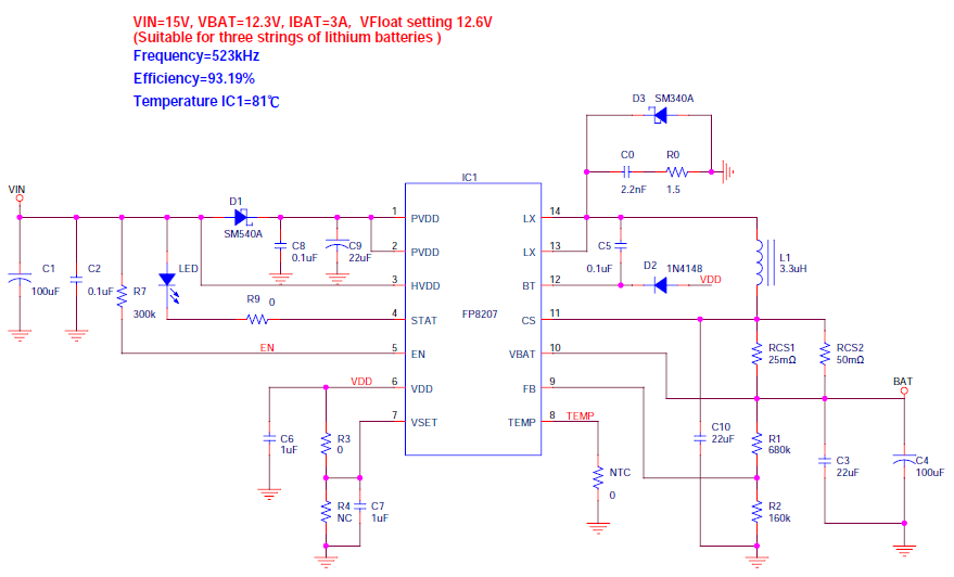
아래와 같은 Application에서 높은 효율 및 Chip 온도를 알 수 있습니다.
VIN=15V, VBAT=12.3V, IBAT=3A, VFloat setting 12.6V (Suitable for three strings of lithium batteries).
-
Efficiency=93.19%
-
Frequency=523kHz
-
Temperature IC1=81℃
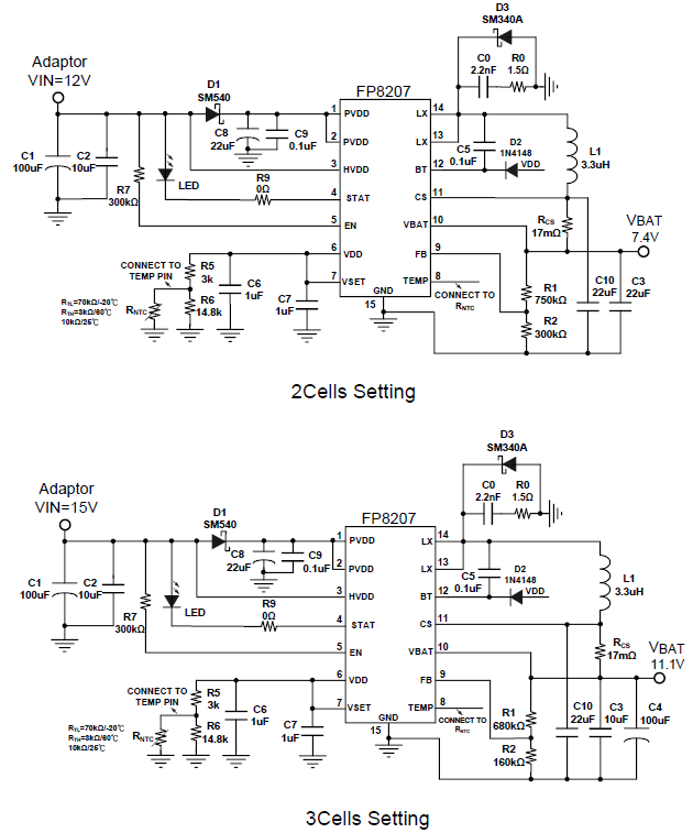
아래는 spec sheet에 있는 응용회로입니다.
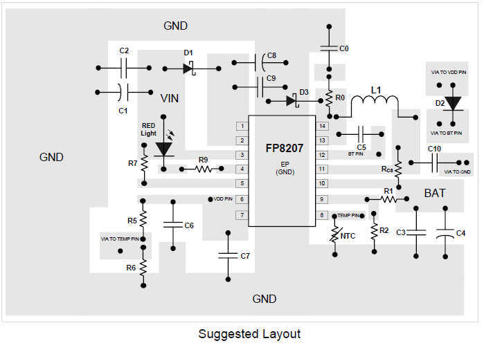
Layout Considerations
1. The power traces, consisting of the GND trace, the LX trace and the battery trace should be kept short,direct and wide.
2. Layout switching node LX, BT and inductor connection traces wide and short to reduce EMI.
3. Place input capacitor C1, C2, C8, C9 nearby Power pin as closely as possible to maintain Input voltage steady and filter out
the pulsing input current.
4. The GND of the CIN should be connected close together and directly to a ground plane.
5. Place RCS nearby BAT pin and CS pin.

'끝없는 Power를 위하여' 카테고리의 다른 글
| FP6153-3A, 36V,Synchronous Step-Down Converter에 대한 고찰 (0) | 2020.12.24 |
|---|---|
| FP6151-5A, 36V, Step-Down Converter에 대한 고찰 (0) | 2020.12.24 |
| DCDC 컨버터(DCDC Converter) (0) | 2020.12.24 |
| FP5217-Non-Synchronous PWM Boost Converter (MOSFET: 30V/8A/15mΩ -peak current 10A)에 대한 고찰 (0) | 2020.12.21 |
| ACDC 컨버터(ACDC Converter) (0) | 2020.12.21 |