오늘은 FP6151-5A, 36V, Step-Down Converter에 대한 고찰을 해 보겠습니다.
FP6151는 High Voltage(HV) input, 5A, 36V, Step-Down Converter로 아래와 같은 특성을 지니고 있습니다.
The FP6151 is a buck regulator with a built in internal power MOSFET. It achieves 5A continuous
output current over a wide input supply range with excellent load and line regulation. Current mode
operation provides fast transient response and eases loop stabilization. A wide switching frequency
range allows efficiency and external component size to be optimized. The device includes under
voltage lockout and thermal shutdown protection. The regulator only consumes 10μA supply current in
shutdown mode. The FP6151 requires a minimum number of readily available external components to
complete a 5A buck regulator solution.
-
Operating Input Range up to 36V(HV)
-
5A Output Current
-
Built-in Soft-Start
-
65mΩ Internal Power MOSFET Switch
-
Up to 90% Efficiency
-
10μA Shutdown Mode Current
-
Adjustable Switching Frequency using external Resistance setting
-
Thermal Shutdown
-
Under Voltage Lockout
-
Internal soft-start: 2ms
-
Available SOP8 With Exposed PAD
Function Description
The FP6151 is a current-mode step-down DC / DC converter that provides excellent transient response with external compensation components.
It regulates input voltages from 4.5V to 36V down to an output voltage as low as 0.808V with maximum 5A load current. And a high-efficiency design with excellent AC and DC performance.
The output voltage is measured at FB through a resistive voltage divider and amplified by the internal error amplifier.
The output current of the transconductance error amplifier is presented at COMP where a network compensates the regulation control system.
The voltage at COMP is compared to the switch current measured internally to control the output voltage.
The converter uses internal n-channel MOSFET switches to step-down the input voltage to the regulated output voltage.
Since the MOSFET requires a gate voltage greater than the input voltage, a boost capacitor connected between SW and BS drives the gate. The capacitor is charged from the internal regulator when the SW pin is low.
Output Voltage (VOUT)
The output voltage is set using a resistive voltage divider from the output voltage to FB.
Oscillator
The oscillator frequency (FOSC) can be set by an external resistor.
Enable Mode / Shutdown Mode
The FP6151 has a dedicated enable control pin, EN. By pulling it high or low, that can be enabled and disabled.
Tie EN to VIN through a 100KΩ resistor for automatic start up.
To disable the part, EN must be pulled low for at least 5us. When floating, EN is pulled up to about 2.0V by an internal 1uA current source so it is enabled.
Boost High-Side Gate Drive (BST)
Since the MOSFET requires a gate voltage greater than the input voltage, user should connect a flying bootstrap capacitor between SW and BS pin to provide the gate-drive voltage to the high-side n-channel MOSFET switch.
The capacitor is charged by the internally regulator periodically when SW pin is pulled to ground. During startup, an internal low-side switch pulls SW to ground and charges the BST capacitor to internally regulator output voltage.
Once the BST capacitor is charged, the internal low-side switch is turned off and the BST capacitor provides the necessary enhancement voltage to turn on the high-side switch.
Thermal Shutdown Protection
The FP6151 features integrated thermal shutdown protection. When the IC junction temperature exceeds +150°C, thermal shutdown protection will be triggered.
The internal power MOSFET is then turned off to limit the device power dissipation (PD).
Once thermal shutdown occurs, this device can go back to normal operation until the junction temperature drops below +140°C approximately.
Application Information
Input Capacitor Selection
The input current to the step-down converter is discontinuous, therefore a capacitor is required to supply the AC current to the step-down converter while maintaining the DC input voltage.
Use low ESR capacitors for the best performance. Ceramic capacitors are preferred, but tantalum or low-ESR electrolytic capacitors may also suffice.
The input capacitor can be electrolytic, tantalum or ceramic.
When electrolytic or tantalum capacitors are used, a small, high quality 0.1μF ceramic capacitor should be placed beside the IC as possible.
When using ceramic capacitors, make sure that they have enough capacitance to provide sufficient charge to prevent excessive voltage ripple at converter input.
Inductor Selection
The inductor is required to supply constant current to the output load while being driven by the switched input voltage.
A larger value inductor will result in less ripple current that will result in lower output ripple voltage.
However, the larger value inductor will have a larger physical size, higher series resistance, and/or lower saturation current.
A good rule for determining the inductance to use is to allow the peak-to-peak ripple current in the inductor to be approximately 30% of the maximum switch current.
Output Capacitor Selection
The output capacitor is required to maintain the DC output voltage. Ceramic, tantalum, or low ESR electrolytic capacitors are recommended.
Low ESR capacitors are preferred to keep the output voltage ripple low.
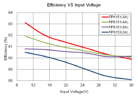
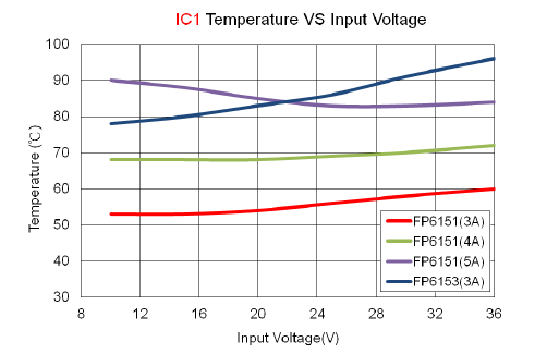
아래는 spec sheet 외의 응용회로, 효율 및 온도 특성 그래프입니다.
실제로 Vin=30V, Vout=5V / Iout=3.5A, Switching Frequency=197kHz 정도로 spec을 정해서 application 하면,
-
Efficiency=87.5%
-
Output Ripple=94mV
-
Temperature IC1=73℃ L1=71℃ D1=89℃입니다.
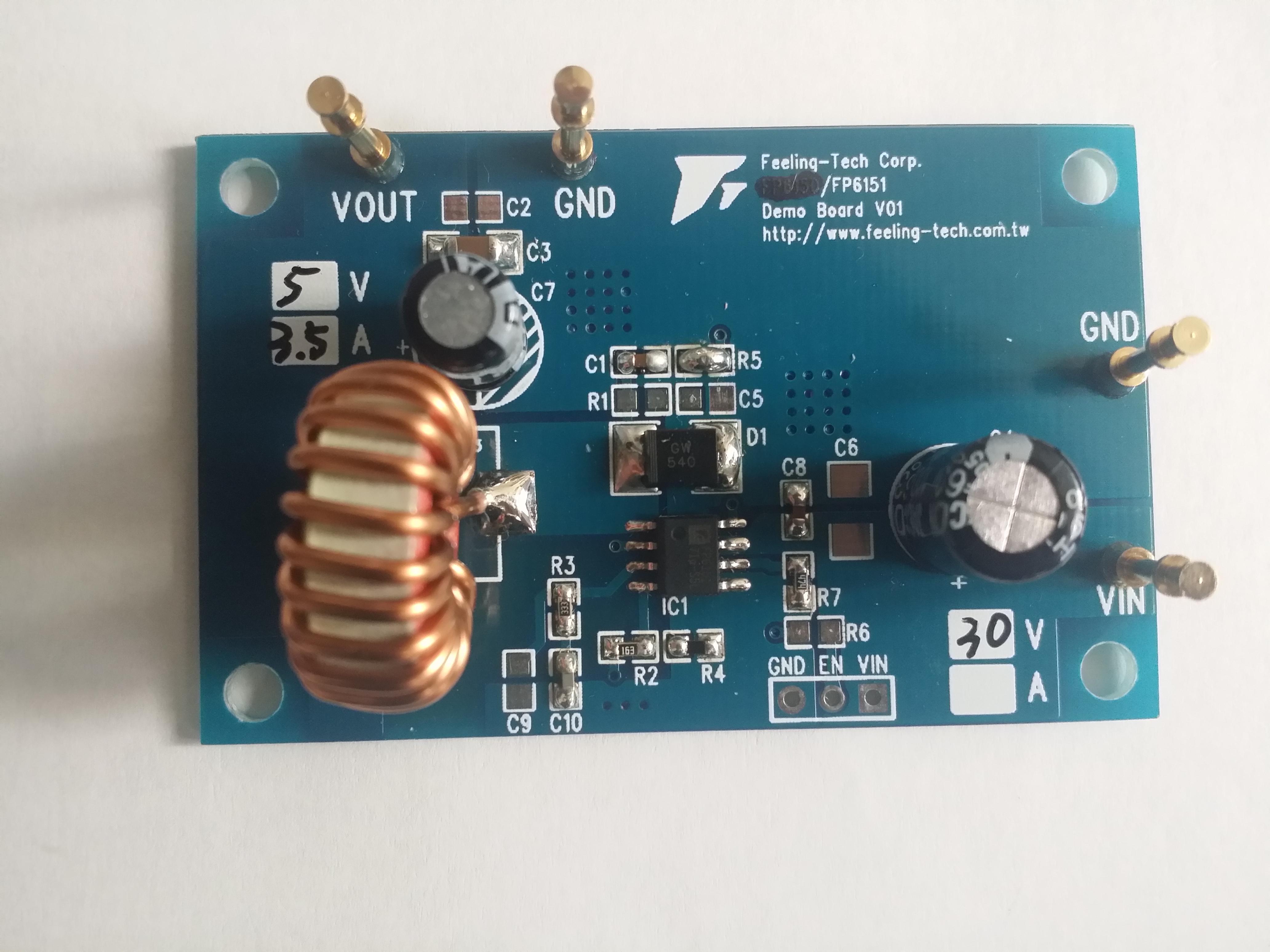
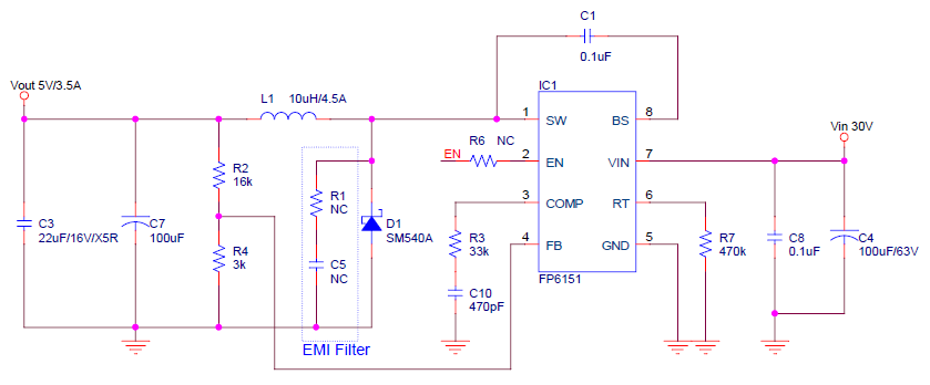
아래는 Spec sheet의 응용회로입니다.

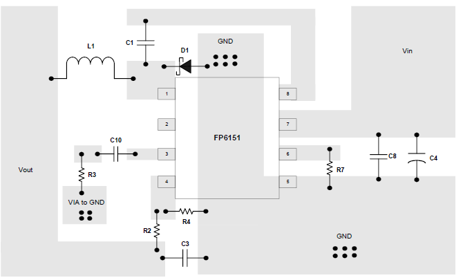
PC Board Layout Checklist
1. The power traces, consisting of the GND, SW and VIN traces, should be kept short, direct and wide.
2. Place CIN near IN pin as closely as possible to maintain input voltage steady and filter out the pulsing input current.
3. The resistive divider R2 and R4 must be connected directly to FB pin as closely as possible.
4. FB is a sensitive node. Please keep it away from switching node SW. A good approach is to
route the feedback trace on another layer and have a ground plane between the top and feedback trace routing layer.
This reduces EMI radiation on to the DC-DC converter’s own voltage feedback trace.

'끝없는 Power를 위하여' 카테고리의 다른 글
| SP687-X2 Capacitor Discharge IC에 대한 고찰 (0) | 2020.12.24 |
|---|---|
| FP6153-3A, 36V,Synchronous Step-Down Converter에 대한 고찰 (0) | 2020.12.24 |
| FP8207-16V 3A Multi-Cell Battery Switching Charger에 대한 고찰 (0) | 2020.12.24 |
| DCDC 컨버터(DCDC Converter) (0) | 2020.12.24 |
| FP5217-Non-Synchronous PWM Boost Converter (MOSFET: 30V/8A/15mΩ -peak current 10A)에 대한 고찰 (0) | 2020.12.21 |